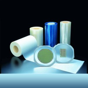
Analysis of PO base material of UV anti-sticking film/wafer cutting film
xinstFeb 27, 2021
UV anti-adhesive film xinst UV-1608 PO film Wafer UV Dicing film substrate UV Dicing Tape is also known as UV loss-adhesive tape and UV anti-adhesive tape. UV film is a kind of UV high-viscosity glue coated on a special PO substrate film. It shows high-strength adhesive strength (1200g~2000g), but the adhesive strength drops sharply after ultraviolet radiation (5g~10g) or even lower or non-adhesive single-sided tape made of special glue.

PO base film is a new type of base film produced by multiple processes from an unstretched polyolefin copolymer film prepared by a casting method. The base film is soft and has outstanding advantages compared with traditional PE film and EVA film on the market. It has super tensile strength and tear resistance. It adopts nanotechnology, multi-process and multi-structure. The surface is waterproof, and the other surface is treated with anti-static corona. There is no precipitate, it is not easy to absorb dust, and achieve the effect of maintaining high light transmission for a long time. It has strong tensile resistance, no dust during cutting, excellent wear resistance and other characteristics, and it is important to have UV protection effect. It is used as the main base film material for UV mucosal film (loss of mucosal film) and OGS acid-resistant film.
UV anti-sticking wafer film and anti-acid film are used in the following industries:
1. Suitable for silicon wafers, tempered glass, electronic components, SMT components, MLCC chip capacitors, chip inductors, positioning and cutting in the manufacturing process, PLC chips, wafers and other semiconductor cutting and manufacturing process protection, EMC or ceramics Substrate LED lamp beads, QFN, PCB, packaged semiconductor chip Package, PLC components, fiber optic head components, wafer LDE chip cutting, quartz glass, mobile phone camera glass, filter cutting, QFN and DFN cutting, etc.;
2. Semiconductor wafer surface processing; electronic and optoelectronic industrial components manufacturing and processing engineering; LCD and TP touch panel glass thinning, grinding and polishing; LED cutting, grinding and polishing; sapphire substrate thinning and grinding process; wafer grinding, cutting, various silicon Chips, packaging substrates, ceramics, glass, crystal fine electronic parts, etc.;
3. PO acid-resistant film is suitable for ITO glass and cover lens chemically strengthened acid etching process protection;
4. Others require high-viscosity and close-fitting protection, and later process protection that is easy to tear off.
Features of UV protective film:
1: High adhesion during cutting, very low viscosity after UV irradiation, the wafer does not fly away and does not remain glue when picking up. Because of the strong adhesive force to fix the wafer, even small chips will not be displaced or peeled off and can be cut reliably.
2: The response time of UV irradiation is fast, which effectively improves the work efficiency. The instantaneous adhesion can be controlled by UV irradiation, and even large chips can be picked up with lighter power.
3. Keep the crystal grains intact during cutting (without any loss of crystal grains) to reduce the breakage produced during cutting.
4. Ensure that the crystal grains will not be displaced or dropped during the normal transmission process, and water will not penetrate between the crystal grains and the tape.
5. Uv cured wafer cutting protective film (the characteristic is that it has an ultra-high viscosity that can not be compared with ordinary protective films before UV curing (can reach an astonishing 1500g-2000g gf/25mm) After UV irradiation, the viscosity can change again It becomes an ultra-low viscosity 15g-20g. Even lower viscosity grams.
6. Another feature is that the PO substrate has extremely strong (horizontal and longitudinal) elongation% (elongation%) that can reach 300 or 600.


